Description
Many products have not been listed yet. For more products, please contact us
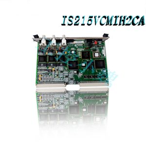
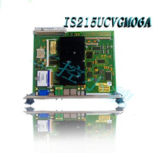
If the product model is inconsistent with the displayed image, the model shall prevail. Please contact us for specific product images, and we will arrange for photos to be taken and confirmed in the warehouse
We have 16 shared warehouses worldwide, so sometimes it may take several hours to accurately return to you. We apologize for any inconvenience caused. Of course, we will respond to your concerns as soon as possible.
VMIVME-4116 332-004116 Other names:
Control board VMIVME-4116 332-004116
VMIVME-4116 332-004116 PLC module
Input/output module VMIVME-4116 332-004116
The unit listed here is VMIVME-4116 332-004116 , which is part of the VMIC converter, CPU, and analog-to-digital drive board series. The VMIC series products were initially developed and produced as materials by General Electric’s Industrial Automation division, but were later acquired and produced by Abaco Systems. Due to another shutdown.
The VVMIVME-4116 332-004116 model is a VMEbus single board computer module based on Intel Pentium Mark III processors. It is equipped with 128 MB of random access memory. There is a standard VME P1 and a VME P2 connector, as well as a VME 64 connector.
The standard components of VMIVME-4116 332-004116 and other VMIC modules in this series are hardware, such as video graphics arrays, keyboard and mouse connection ports, a pair of serial communication ports, a pair of USB ports, and a pair of Ethernet interface connections.
The processor of the VMIVME-4116 332-004116 module can provide up to 256 KB of advanced data transfer cache, utilizing a dual independent bus architecture for high bandwidth and performance.
VMIVME-4116 332-004116 adopts the latest Intel chipset technology, 855GME. This chipset adopts a different architecture (AHA) from the previous generation devices by using a new advanced hub. AHA allows for improving system performance by separating many high bandwidth I/O accesses (such as IDEs or USB devices) from PCI, alleviating bottlenecks on the PCI bus. In addition, the 855GME chipset brings a new level of integration to the motherboard chipset and provides additional features superior to other chipsets. The Hance Rapids I/O Controller Hub (ICH) contains input/output ports for VMIVME-4116 332-004116, or the controllers that drive the rest of the I/O are connected. It includes support for two external PCI buses (32-bit 33MHz and 64 bit 66MHz), four USB ports, DMA controller, two 16550 serial ports, real-time clock, interrupt controller, and watchdog timer.
I/O port mapping
Like desktop systems,VMIVME-4116 332-004116 includes special input/output instructions to access I/O peripherals residing in the I/O addressing space (independent and distinct from the memory addressing space). The location in the I/O address space is called a port. Therefore, the CPU includes an independent 64K byte I/O address space, which can be accessed as bytes, words, or long words. The standard hardware circuit only retains 1024 bytes of I/O address space from it. The I/O of peripheral devices ranges from $000 to $3FF. All standard PC I/O peripherals, such as serial and parallel ports, hard and floppy drive controllers, video systems, real-time clocks, system timers, and interrupt controllers, are addressed in this area of the I/O space. BIOS correctly initializes and configures all these registers; Adjusting these I/O ports usually does not require direct use.
System Interrupt
In addition to the I/O port address, I/O devices also have a separate hardware interrupt line allocation. The 256 vector interrupt table from $000000 to $003FF in the corresponding interrupt vector memory is assigned to each interrupt row. 16 people can wear masks to interrupt and single non masked interrupt (NMI) are listed in Table 2-3 and their functions. Table 2-4 on page 41 provides a detailed explanation of the vector table in interrupt vectors. The interrupt numbers in hexadecimal and decimal are also defined as real numbers and the protection mode in Table 2-4 on page 41. The interrupt hardware implementation onVMIVME-4116 332-004116 0 is built around the PC architecture evolved from IBM PC/XT. In the IBM PC/XT computer, there are only eight interrupt request lines numbered IRQ0 to IRQ7 at PIC. The IBM PC/AT computer has added eight additional IRQx lines, with the second PIC cascaded from IRQ8 to IRQ15 to the original main PIC photo. The IRQ2 at the main PIC is submitted as a cascaded input from the secondary PIC. The architecture is shown in Figure 2-1 on page 46. In order to maintain backward compatibility with PC/XT systems, IBM chose to use the IRQ9 input from PIC as a disconnected extension bus in the old IRQ2 on PC/XT. Therefore, in the AT system, the IRQ9 interrupt line is connected to the pin (pin B4) on the old IRQ2AT expansion bus (or ISA bus).
Dual Ultra 160 SCSIs
The dual 160 SCSI interface of VMIVME-4116 332-004116 makes the unit an ideal choice for embedded applications, especially those with standard hard and floppy disks that cannot use the drive. The VMIVME-4116 332-004116 dual channel Ultra160 SCSI host adapter includes LSI logic LPC53C1000, a highly integrated PCI single channel Ultra160 SCSI controller. LPC53C1000 is 100% compatible with the Ultra160 SCSI program, providing additional features to ensure stable operation of the Ultra160 system. Fast SCSI, LPC53C1000 supports Ultra SCSI, Ultra2 SCSI, and Ultra160 SCSI. The dual conversion clock achieves a throughput of up to 160 megabytes without increasing the interface clock speed. LPC53C1000 uses the same CRC algorithm channel as FDDI, Ethernet, and fiber, and detects unit errors, dual bit errors, odd errors, and all burst errors up to 32 bits. Provide complete end-to-end protection I/O for SCSI, AIP protects all non data stages, and enhances the CRC function of Ultra160. SureLINK domain validation technology detects the configuration of the SCSI-bus and automatically tests and adjusts the SCSI-transfer rate to optimize interoperability. The LPC53C1000 controller and Ultra160 provide basic (level 1) and enhanced (level 1, level 2) domain validation, while the LPC53C1000 adds marginalization functionality (level 3) domain validation. The PCI interface Ultra160 SCSI complies with the revised version 2.2 of the PCI local bus specification and implements a 64 bit/66MHz PCI bus. LPC53C1000 complies with PCI Power Management Interface Specification Revision 1.1 and PC 99, supports power status D0, D1, D2, D3hot, and D3cold, power management function registers, as well as programmable values for PCI subsystem vendor ID and subsystem ID. Extended access cycle (memory read line, memory read multiple, memory write and Invalidate).
The BIOS of LPC53C1000 in Ultra160 SCSI memory is located in the system BIOS. The serial 2-wire interface provides a connection to the external serial EEPROM for storing subsystem supplier IDs and subsystem IDs. The Ultra160 SCSI processor LPC53C1000 provides an Ultra160 SCSI controller on a single chip. The controller supports up to 160 megabytes of Ultra160 SCSI synchronous transfer rate on the LVD on the SCSI bus. The integrated LVDlink transceiver supports both LVD and single ended signals without the need for an external transceiver. Fast, Ultra, Ultra2, and Ultra160 SCSI are all supported by LPC53C1000. The on-chip SCSI clock quadrupler allows the chip to achieve an Ultra160 SCSI transmission rate with a frequency of 40MHz through input. The 8 KB internal RAM used for SCRIPTS instruction storage allows all access to be kept internally, reducing time spent on the PCI bus. A. The 944 byte DMA FIFO on each channel allows the device to effectively burst bytes onto the 512PCI bus. The phase mismatch of the SCSI bus is processed in SCRIPTS, thereby reducing CPU utilization..jpg)
Ultra160 SCSI terminal
Each end of all SCSI-buses requires a terminal network to function properly. The specific termination requirements vary depending on the type of SCSI device on the bus. The SCSI host adapter uses UCC5630A terminal IC to automatically sense the SCSI bus and switch the terminal to any single ended (SE) or low-voltage differential (LVD) SCSI, depending on the type of device connected to the bus. UCC5630A terminal IC is used for multi-mode active terminal applications, where SE and LVD devices may coexist. UCC5630A has SE and LVD terminal network components integrated into a single chip, and the correct network is automatically determined by the SCSI-bus for the “DIFSENS” signal. The SCSI-bus DIFSENS signal line is used to identify which types of SCSI-devices exist on the bus. After connecting the power, the UCC5630A DIFSENS driver will attempt to provide 1.3V voltage to the DIFSENS line. If only LVD devices exist, the DIFSENS line will successfully drive to 1.3 V and the terminal will be configured for LVD operation. If any single ended devices exist, they will experience a short circuit to ground on the DIFSENS line and send a signal UCC5630A configured in SE mode to accommodate SE devices. Alternatively, if there are any High Voltage Differential (HVD) devices present, the DIFSENS line will be pulled up and the terminator will enter a high impedance state, effectively disconnecting from the bus.
All products on this website are special products, and market prices have been fluctuating,
The specific customer service quotation shall prevail, as the product is a new product and the price is not genuine,
Please confirm the model, product, price, and other detailed information with customer service before placing an order. The website has been used,
The new one is for sale, please contact customer service to communicate.
Warehouse discount product recommendation:
VMIVME-7698–140
VMIACC-5595–208
VMIACC-5595–208
VMICPCI-7806–211000
VMIPMC-5565
VMIVME-2540–300
VMIVME-4140–000
VMIVME-3215–000
More……


-100x100.jpg)
-300x300.jpg)


Reviews
There are no reviews yet.